5.30.2007

COMPANY: Nanoident Technologies

Overview
Nanoident Technologies is a privately held company founded in 2004 out of Austria with the aim of printing semiconductors, biometric assays, and photonic lab-on-a-chip systems with a method similar to that utilized by nanosolar. Nanoident has two major subsidiaries. The Austrian-based Nanoident Biometrics prints biometric sensors for security purposes, while Bioident Technologies, based in Menlo Park, CA, prints opto-electronic capabilities on lab-on-a-chip systems for diagnostics. Details on the financial investments made into Nanoident are unknown, but CEO Klaus Schröter claims to have received no venture capital money to fund R&D.

www.Nanoident.com


Subsidiaries
Bioident Technologies- Bioident prints opto-electronic capabilities on semiconductor based photonic lab-on-a-chip systems for detection of biological agents in food, water, and blood or tissue samples for diagnotic purposes. Bioident's technology integrates microfluidic lab-on-a-chip systems with printed light emitting and detecting electronic interfaces to create a novel platform in which samples can be easily illuminated and detected in real time for detailed analysis.

Nanoident Biometrics
- Nanoident biometrics prints biometric sensors for use in identification softwares. Nanoident's biometric sensor are printed for touch screening, and test for fingerprints as well as blood and skin parameters on the surface of the finger. Nanoident seeks to use this technology
in next generation wireless and internet communication, payment systems, as well as other identification solutions.

Products
Semiconductor 2.0- This is Nanoident's platform for printed semiconductor-based products. This printing process allows for custom designed devices to be produced at a fraction of the cost as traditional semiconductor fabrication plants.

PhotonicLab- This platform enables real-time, in-situ and multi-parameter detection and analysis capabilities for lab-on-a-chip systems. The technology improves on the capabilities of traditional lab-on-a-chip technology while maintaining the cost-effectiveness inherent in the technology.

News
3.08.2007- Bioident receives the 2007 Frost & Sullivan enabling technology of the year award

3.08.2007- Biodent announces first complete lab-on-a-chip system based on printed semiconductor technology

3.13.2007- Nanoident opens first manufacturing plant for printed opto-electronic semiconductor sensors

9.18.2006- Bioident technologies opens U.S. headquarters in Menlo Park, CA

6.26.2006- Nanoident announces its biometrics division

11.28.2005- Nanoident builds the world's first factory for organic semiconductor sensors

10.10.2005- Nanoident wins the coveted Austrian Innovation award

6.30.2005- Nanoident presents first high resolution photodetector based on organic semiconductors

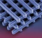
(FIGURE from Nanoident.com)

5.22.2007

TECHNOLOGY: Lab-on-a-chip

Lab-on-a-chip technology is superficially similar to traditional microchips. They are currently sketched on silicon surfaces and consist of many micro- or nanosized connections. However, rather than passing electric current across these connections, lab-on-a-chips are designed to transmit and mix fluids for scientific assays. These chips can be used in detection assays in cells for viruses, bacteria, or cancer, and may soon be used to test the physiological responses of patients to new medicines.

This technology utilizes principles from micro- and nanofluidics. On this scale, fluids behave differently than they do on a more macro level, especially regarding movement. Rather than using physical force to guide the fluids, techniques involving electrophoresis and electroosmosis must be used. Electrophoresis is accomplished by applying a voltage difference across a channel connecting fluids. The voltage difference interacts with ions within the fluids to push the fluids across as needed. Electroosmisis, however, involves charges on the wall of connectors that interact with ions at the outer surface of the fluid to push it along the channel. Both methods are electronic by nature, making these chips conducive to automation using software protocols.

Lab-on-a-chips are advantageous in their ability to save a lot of space and personnel for research laboratories. By automating tasks, the chips reduce the need for technicians to conduct the experiments. Furthermore, the size of these chips make it possible to run orders of magnitudes more assays simultaneously in a given lab. Lab-on-a-chips should reduce the cost and efficiency of running experiments. However, there are still issues with this new technology. Micro- and nanofluidics are not completely understood, making it more difficult to manipulate fluids at this level. While lab-on-a-chip technology is promising, progress has been slower than expected as developers have struggled to understand the behavior of fluids on the micro- and nanoscale.

(FIGURE from Agilent.com)

4.23.2007

Russia Pledges $1B to Nanotech Research

Last Wednesday President Vladimir Putin announced a $1B initiative to fund nanotech research and aid companies with investments in the science. The money would also help transform the Kurchatov nuclear institute into the hub for Russian nanotech research. The initiative stems from Russia's massive oil and gas export and is intended, according to Minister Sergei Ivanov, to diversify an economy now heavily dependent on raw materials. The money is in addition to the approximately $5.8B that Russia has already devoted to nanotech research.

Ivanov, who will head the budgeting of the nanotechnology initiative, predicted that 90% of the money will go to fund civilian applications, with the rest going toward the military. Putin added that “No doubt, nanotechnologies will become a key industry for the creation of ultra-modern and ultra-effective offensive and defensive weapons, as well as means of communications.”

This last quote certainly compels concern, especially given the strained relations between the United States and Russia as of late. With all the attention being given to the health concerns of domestic nanotechnology manufacturing, it seems that the threat of nanotech-enabled weaponry has been overshadowed.

Below are some links to articles regarding nanoweapons:

CRNano.com
Janes.com
Newsmax.com

4.20.2007

TECHNOLOGY: Nanorust

Water purification has become a major issue in third world countries, where thousands of people die each year from arsenic contamination in their drinking water wells. A lab at Rice University recently published an article in Science magazine describing small crystals containing Fe3O4 rust particles dubbed "nanorust", which may prove to be an answer to low-cost and effective water purification in these countries. These nanorust crystals serve as another example of how the unique properties of nanoscale materials can be applied in today's industries.

A general principle of magnetics states that as particles get smaller, the amount of magnetic force required to move the particles increases. This relationship is due to the fact that magnetic power is proportional to the volume of the material acted upon, so when particles get too small their magnetic power potential falls below the threshold required to overcome initial inertia. A lab at Rice led by Dr. Vicki Colvin sought to test this principle on the nanoscale and found that, after reaching a critical threshold of approximately 50 nm, it becomes easier to manipulate the materials. This, they propose, is due to the fact that at this miniscule size, the particles exert forces on each other in a cooperative manner that allows for magnetic separations with even weak handheld magnets.

After proving this concept of nanoscale separation, Dr. Colvin's lab tested the potential of this method to remove arsenic from drinking water. Taking advantage of the tendency of rust to bind arsenic, the lab found that adding nanorust to water and applying a magnetic field effectively removed the arsenic and purified the water enough to meet EPA standards.

The benefits of this method of magnetic separation over traditional separation methods such as centrifugation and filtration are a few fold. The process is not only more selective and efficient than its counterparts, but it may also turn out to be a much cheaper method. While Dr. Covlin admits that the process is too expensive to currently use in water filtration, they claim to be working on methods that will eventually produce nanorust at a very low cost and scalable level.

(FIGURE from TechnologyReview.com)

4.16.2007

COMPANY: Nanophase

Overview
Nanophase was founded in Romeoville, IL in 1989 and is currently publically tra
ded with a market cap of $130M. Nanophase is one of the first companies founded in the nanomaterials field and specializes in manufacturing metal-oxide powders for use in a wide variety of applications, including personal care, semiconductors, optics, and environmental catalysts. Nanophase's business model relies on partnerships with businesses in target markets. Nanophase's current exclusive partnerships with BASF, Rohm, and Haas Electronic Materials brought in $9M in revenue in 2006, and is reporting first quarter revenues of $2.9M in 2007, representing a year-over-year growth of 45% - the highest in the field.

Nanophase.com

Technology
Nanophase produces nanocrystalline powders containing nanoscale grains with properties capable of enhancing the performance of other materials. Nanophase has produced powders designed to enhance the chemical, mechanical, electrical and optical behavior of materials. Nanophase has combined methods of Physical Vapor Synthesis and Nanoarc Synthesis with a patented polymer coating to manufacture a variety of nanocoatings, including some that are compatible with fluids - a feat unmatched by current competitors.

Applications
Antimicrobial- Powders have been developed with antimicrobial properties to aid in the preservation of certain materials including wood, plastics, textiles, and materials subjected to harsh conditions.

Catalysts- Nanomaterials can be used as catalytic converters for more efficient emissions in fuels or for the creation of fuel cells.

Performance Coatings- Powders can be used as coatings to dimish the effects of UV rays, static charge, and general abrasion on materials.

Personal Care- Nanomaterials can be used as sunscreens, deodorants, dental coatings, and antibacterial coatings in personal care products.

Polishing- Nanophase's uniquely blended polishes can be used for high-quality semiconductor or glass polishing.

Products
For a list of Nanophase's products, see their catalog.

Collaborations
BASF- Nanophase partners with BASF for sunscreen and personal care applications.

Rohm & Haas- This partnership is largely for semiconductor applications.

BYK Chemie- For coatings and ink applications.

Alfa Aesar- For research sample distribution.

(FIGURE from NSTI.org)

4.12.2007

TECHNOLOGY: Nanogenerator

Much of the buzz surrounding nanotech has been centered around the prospect of nanoscale devices. Nanotech pundits theorize that these devices will serve as "smart molecules", building nanostructures and treating diseases on their own power. Before these nanodevices can be used on a mass scale, however, a nanoscale power source must be developed. There are two major requirements that this power source must fulfill. First, it must be small enough that it maintains the nanoscale size advantage of the device after it is coupled with that device. Second, these devices must be able to generate power from their immediate surroundings.

Scientists from the Georgia Institute of Technology recently published an article in Science detailing the creation of a nanoscale generator (see figure 1) capable of ge
nerating power from environmental phenomena such as ultrasonic waves, mechanical vibrations, and even blood flow. These generators consist of zinc-oxide nanowires (nanowires are nanotubes made out of elements other than carbon) which create charges based on their movements in relation to a jagged silicon electrode plate (see figure 2).

The nanowires are moved by environmental forces such as waves or vibrations, which cause charge to be transfered from the wires to the electrode. This transfer of charge can create a current on the level of nano-Amps which, with further optimization, could lead to up to 4 watts of power delivered per square centimeter.

These nanogenerators are non-toxic and represent a large step in the development of nanoscale "smart molecules". Imagine drugs that live in your body and work to not only cure ailments, but maintain the body and prevent potential ailments as well. These generators could provide the power necessary for such long term pharmaceutical action.

(FIGURE 1 from HipTechBlog.com, FIGURE 2 from Science article)

4.04.2007

COMPANY: Arrowhead Research

Overview
Arrowhead Research Corporation is a publicly traded company based in Pasadena, CA with a market cap of around $160M. Arrowhead focuses on developing nanotechnology with sponsored research grants to top institutions and through research and development within its subsidiary companies, Aonex Technologies, Insert Therapeutics, Calando Pharmaceuticals, and Unidym. Arrowhead's business plan involves commercializing nanotechnology products owned by its subsidiaries, funding nanotech R&D in exchange for licensing rights, and acquiring IP for nanotechnologies.

Subsidiaries
Aonex Technologies- Specializes in nano-enables semiconductor fabrication to reduce costs, improve performance, and integrate multiple functions into a single device. The technology under Aonex has many applications in electronics, but the major focus is currently on next-generation solar cells.

Insert Therapeutics- Couples its patented delivery technology, Cytosert, with drugs for improved drug solubility, stability, circulation, and targeting for enhanced safety and efficacy. The cytosert linkage lengthens the drug combination and, through the enhaced permeability and retention (EPR) effect of tumor cells, prevents loss of drug by normal vessel leakage while enhancing drug accumulation in targeted tumor cells.

Calando Pharmaceuticals- Utilizes the phenomenon of RNA interference (RNAi) to “silence” the expression of disease causing genes. While the RNAi technology is rather widely used, Calando uses self-assembling nanoparticles to prime the drug for intravenous injection. Preclinical studies on this polymer-RNAi combination have been promising.

Unidym- Uses carbon nanomaterials (buckytubes and buckyballs) in the development of next-generation electronics. The technology is based on networks of carbon nanotubes, leading to high electrical conductivity, mechanical flexibility, transparency, and environmental resistance. Initial products include transparent and electrically conductive films that offer competitive alternatives to indium tin oxide (ITO) in applications such as flat panel displays, touch screens, and solar cells.

News
1.25.2006- Arrowhead receives $19.6M in institutional investments from York Capital Management and Knott Partners in exchange for stock.

1.10.2006- Arrowhead is selected for inclusion in the Powershares Lux Nanotech Portfolio, which is intended to track a group of leading companies involved in developing and manufacturing nanotechnology.

C
ollaborations
6.14.2006- Arrowhead acquires nanoelectronics company Unidym for $7M

2.22.2005- Arrowhead launches Calando Pharmaceuticals as a majority-owned subsidiary to develop new technology taking advantage of RNAi technology

4.02.2007

TECHNOLOGY: Buckyballs

Buckminsterfullerenes, or buckyballs as they are more commonly known, are the spherical equivalent to carbon nanotubes. The carbon lattice in buckyballs consists of pentagonal carbon chains surrounded by hexagonal chains in a pattern much like that of a soccer ball (see figure). This pattern allows the carbon lattice to bend in a way that is most stable in a hollow spherical form.

The most immediately apparent contributions that these buckyballs may make lie in the field of drug delivery and transport within the body. Currently, liposomes are used to transport drugs through the body for a slower acting and longer lasting effect with better localization to target areas. These liposomes can be introduced through many different methods, including inhalation. However, these liposomes are often targeted by killer cells in our immune system and tend to be cleared from lung tissue very quickly, decreasing the effectiveness of the drug.

Buckyballs have recently been proposed as a potential replacement for liposomes in this type of drug delivery. The superior biological stability of buckyballs allows them to be retained in the lung much longer than liposomes for better drug delivery. Moreover, the simple lattice structure of these buckyballs make it easy to attach multiple drugs to the system, allowing for drug cocktails designed for more complicated action on target sites. A recent article published in the JACS demonstrated that when coupled with cancer drug, Paclitaxel, these buckyballs show an ability to remain in the lung longer than traditional liposomes.

A lab in Cornell is currently researching a method of creating buckyballs out of DNA molecules, and several other labs are working on further potential uses for these balls. Further applications include uses as molecular ball bearings, optical devices, and semiconductors.

3.20.2007

TECHNOLOGY: Laser Nanomachining

While the nanomaterials and devices developed in nanoscience labs hold a great deal of promise in their future applications, scalability remains an issue. The jump in quantity of nanomaterials required in basic research to that required for mass scale manufacturing is a formidable one. In fact, one of the largest obstacles on the path to bring progress in nanoscience to mainstream markets is that of manufacturing. A recent paper published in PNAS offers a potential solution in a method of machining with ultra-fast laser pulses that can carve into materials with precision on the order of nanometers.

In their paper, this group, led by Dr. Alan Hunt from University of Michigan, found that by using laser pulses on the order of femtoseconds (1 millionth of a nanosecond), they could carve holes and canals (see figure) in metals nanometers wide while doing very little damage to areas outside the target zones. This method of carving involves freeing up electrons with each laser pulse and accelerating them to tunnel through the material, exciting electrons that they encounter on the way in what is described as an "avalanche effect". The extremely short pulse durations used in the experiment constrict this effect to within target zones and result in cuts which appear smooth down to 4nm resolution.

This laser nanomachining has a wealth of applications in the nanotech industry. Its speed and ease of manipulation far outmatch the capabilities of current methods of nanolithography. Laser nanomachining will most likely find a niche in electronics industries for its promise as a nanoscale mill. Its foreseeable applications are destructive (as opposed to constructive layering of nanomaterials), and carving will probably be the largest role for this technology. Laser nanomachining provides speed and manipulation similar to that of traditional milling and will likely serve similar purposes - albeit on a nanoscale.
(FIGURE from article)

3.15.2007

TECHNOLOGY: Microneedles

When oral medications fail due to failed absorption, poor dosing, or degradation in the GI tract, injections are the most common alternative. However, injections are not the most appealing method of drug delivery from a marketing standpoint. Almost 30 years ago, transdermal patches were developed as a noninvasive alternative to injections, though low absorption through the skin has limited these patches to select compounds such as nicotine and steroids. Enter the microneedles - micron sized needles capable of delivering drugs beneath the skin with the absorptive powers of injections and without their painful pricks.

One might ask, why must we deliver nanometer sized drugs through millimeter sized needles? There is no reason for this size disparity in most cases, and microneedles hold the promise of drug injection at a fine level that bypasses our nerves and saves us from the dreaded prick feeling. Feats in microengineering have finally led to reliant manufacturing of these microneedles to the point where several labs across the country have been able to test these needles in animal models fot the delivery of traditional injection medications like insulin.

The most common method through which these microneedles have been used is through a patch attached to the needle array. Once the patch is placed over the body, the needes can penetrate the shallow layers of skin and commense the injection of drugs. The actual injection can be controlled in a number of ways, from simple diffusion to iontophoresis to polymer control. In iontophoresis, an electrical gradient causes the drug molecules to move in a desired direction. This can be controlled through electric systems on the patch for time control of drug release. Polymers are complex proteins used in drug delivery systems that can act to release drugs due to a timing mechanism or action from external cues.

Today, microneedles can be microfabricated into many designs from many materials including silicon and metal. Studies have shown that patches covered with these needles cause no pain and are, in fact, indistinguishable from normal patches by human subjects. The needles have already been proven successful in animal models and may someday help provide much preferable solutions to injection for medications like insulin.

(FIGURE from mems.gatech.edu)

3.08.2007

COMPANY: Nanosys

Overview
Nanosys is a privately held company founded in 2001 in Palo Alto to develop nanomaterials for a wide variety of industries, including energy, biotech, and electronics. The technology under Nanosys is covered by over 500 patents, and Nanosys has secured partnerships with many industry leaders, including Intel, In-Q-Tel, NTT DoCoMo, Rockwell Collins, the Sharp Corporation, and the U.S. government. In essence, Nanosys is a company fueled by a rich ecosystem of Nanotech-savvy engineers and business partners that provides nanoscale innovation in high technology industries. Nanosys has received awards from Red Herring magazine, Small Times magazine, Scientific American, and the World Technology Network, and has received over $125M in funding from venture capitalists, private equity firms, and the government.

NanosysInc.com

Technology
The core technolgy of Nanosys involves piecing together materials atom-by-atom with elements such as Silicon and Gallium with an aim toward maximal control over composition, size, shape, and surface chemistry. As we have seen in earlier technology profiles of nanoshells, dendrimers, and nanotubes, the functional characteristics of a material can be largely dependent on the tiniest manipulations of its matter. Such manipulations can produce a wealth of desirable characteristics in a material such as superconductivity, biological specificity, and unparalleled strength. Nanosys has taken advantage of these properties of nanoscale materials to produce and patent a plethora of new materials with properties that are currently and will continue to remain very valuable in high technology manufacturing.

Products
While Nanosys does not have any products that it considers its own, it has utilized partnerships with industry leaders to develop a range of interesting technologies including flexible electronics, non-volatile memory, fuel cells, solar cells, and nano-surfaces for use in biological assay systems.

News
4.12.2006- Nanosys receives $4.6M in government contracts

11.9.2005 - Nanosys raises $40M in private equity financing led by El Dorado Ventures

5.12.2005 - Nanosys named a Top 100 company by Red Herring magazine

10.12.2004 - Nanosys Wins 2004 World Technology Network Award

12.1.2003 - Nanosys founders selected as top nanotechnology researcher and business leader finalist by Small Times magazine's 2003 Best of Small Tech

11.19.2003 - Nanosys named business leader in nanotechnology and molecular electronics on the "Scientific American 50"

Collaborations
3.6.2007- Nanosys collaborates with Rockwell Collins for development of a nanotechnology enabled optical system

1.11.2007- Nanosys, DoCoMo Capital, and NTT DoCoMo collaborate on the roles of nanotechnology enabled wireless communication

10.11.2005- Nanosys and Sharp expand a collaboration to develop fuel cells to include nanotechnology enabled displays

8.22.2005 - Nanosys and In-Q-Tel expand collaboration to develop nanotechnology enabled phased array antennas for the government

1.14.2004 - Nanosys and Intel collaborate to investigate nanotechnology enabled memory

2.28.2007

TECHNOLOGY: Artificial Nano-Nerves

Over half a century ago, scientists discovered that the neurons in our brain use electrical signals to communicate and process information. Since that time, there has been a fascination with the possibility of using electrical stimulation to control brain processing - especially in cases where brain damage has left individuals with disabilities. Recent advances in labs at the University of Texas Medical Branch at Galveston (UTMB) and the University of Michigan have shown how nanoparticles may help bring significant advances in this so-called field of brain "prosthetics".

This process, which was published in an article in Nano Letters, involves placing many layers of ultra-thin films of mercury-tellurium (HgTe) coupled with positively charged polymer called PDDA, on a plate and coating the layers with materials designed to couple with a receiving neuron. When light of a certain wavelength hits the film, the HgTe compounds shoot electrons into the PDDA layers, producing an electrical current (see figure). This current can then be transferred into the connected neuron to create a neural signal, also known as an action potential.

One of the major advantages of this system is its "wireless" nature. Without a need for wires, these particles add a flexibility that may someday prove very useful in creating prosthetic limbs capable of responding to signals from our own brains. In addition, the responsiveness of these devices to light make them prime candidates for potential creation of artificial retinae. By tuning each device to a certain wavelength of visible light, scientists may someday be able to simulate color vision in a form transmittable to the brains of the blind or color blind.

(FIGURE from the article)

2.24.2007

COMPANY: Illumina, Inc.

Overview

Illumina, a publicly traded company since 2000, was founded by scientists at Tufts University in Boston in 1998 after their invention of a BeadArray technology useful for genetic assays. Illumina’s mission is to develop technology capable of large-scale analyses of genetic variation and function, which may provide crucial information necessary to create individually personalized medicine. Unlike traditional medicine, which relies on the treatment of observable symptoms, personalized medicine uses information of the genetic makeup of individuals to determine their risk to diseases and succeptability to the cures or side effects of a drug. Illumina looks to capitalize on this trend of genetically personalized medicine and provide genetic diagnostic tools at a high quality level. Illumina earned $40M of gross profit from $185M in revenue in 2006 and was named as Forbes fastest growing tech company.

Illumina.com

Technology

Illumina's original assay system is the BeadArray technology assay (shown in figure). In this assay, small 3 micrometer silica beads containing hundreds of thousands of nucleotide sequences self-assemble onto slides and bind DNA or RNA. This array system can be used to genotype DNA or RNA to determine a patient's genetic predispositions to certain diseases.

The solexa sequencing system was also developed by Illumina as a tool for sequencing DNA samples. The system captures DNA fragments and amplifies them a considerable amount before determining their sequence through use of multicolored fluorescence tags coordinated to specific bases of the DNA. These technologies can be used to determine the health profiles of patients as well as to determine the biomarkers that may predict a potential drug's efficacy or toxicity. Thus this personalized medicine technology is both geared directly towards patients and towards the development of drugs that may cure diseases in the future.

Products
Illumina has a large array of products. Here are some of the most prominent ones:

Beadstation 500- This system uses the BeadArray technology to perform genetic assays on samples of DNA or RNA.

Beadlab 1000/2000- These systems are used for very high throughput assays capable of creating around 1 million genotypes per day.

Genome Analyzer- This system uses a parallel processing approach to sequence gene fragments at a very high throughput level.

News
7.1.2000- Illumina IPOs and raises over $100 million.

12.1.1999- Illumina closes a $28 million Series C financing.

11.1.1998- Illumina receives an initial round of funding of $8.6 million to develop their core technology


Collaborations
11.1.2006- Illumina acquires Solexa, the leading genomic-scale sequencing technology, in a stock-for-stock merger of 0.334 Ilumina stock for each Solexa share.

4.11.2005- Illumina announces the completion of its acquisition of CyVera Corporation for $17.5M in both stock and cash. CyVera is the developer of the VeraCode technology that Illumina uses.

FIGURE from Illumina.com

2.21.2007

Directory

Below is a directory of the posts that I have written sorted by class and listed alphabetically. I will update this list as I add posts to the blog. Feel free to post comments here with any general questions or comments not related to my other posts.

Technologies
Buckyballs-Carbon lattice balls with many uses, including drug delivery
Dendimers-Branched carbon polymers with a variety of uses in biotechnology
Lab-On-A-Chip-Small chip allowing for mizing and processing of materials through nano-sized channels
Laser Nanomachining-An ultrafast laser capable of serving as a nanoscale mill
Microneedles-Microsized needles capable of injecting drugs through patches
Molecular Memory-A memory based on bistable molecules connected by nanoscale wires
Nanogenerator-A nanosized generator harnessing energy from ultrasonic waves
Nanolithography-A method for "writing" molecules onto a template in an organized fashion

Nanonerves-Light induced electrical signaling used in nerve stimulation
Nanorust-Nanoscale rust particles used with magnetic force to purify water
Nanoshells-Gold particles used for nanoscale detection whose optical properties are based on size

Nanotubes-Tubes of carbon lattices with amazing strength, flexibility, stability, and conductivity
Protein Scaffolds-Self assembling scaffolds used to repair damaged tissue
Quantum Computing-Quantum mechanical computers capable of parallel processing

Companies
Arrowhead Research-An umbrella company with subsidiaries harnessing nanotechnology
Illumina-An innovator in genetic analysis systems for use in personalized medicine

Nanoident-Utilizes nano-printing techniques to print diagnostic chips and biometric sensor assays
Nanophase-Provides nanocrystalline powders for a variet of applications
Nanosolar-Uses innovative system of printing thin film solar cells for cheaper and more efficient solar power

Nanospectra-Uses nanoshells for imaging, targeting, and ablation of cancerous tumors
Nanosphere-Uses gold nanoprobes to detect proteins, DNA, and toxic substances
Nanosys-Builds and develops nanosolutions for high technology companies
Oxonica-Nano-based company with subsidiaries in energy, healthcare, materials, and security
PowerMetal Technologies-Uses coat of nano-size metal grains to strengthen sports equipment

Starpharma-A leader in dendrimer incorporation into drugs including a gel for STD prevention

News
4.23.2007-Russia pledges $1B to nanotech research
2.06.2007-UN calls for tighter nanoparticle regulations

2.20.2007

TECHNOLOGY: Quantum Computing

Neurons in the human brain can muster out about 1000 operations per second - many orders of magnitude slower than the trillions of operations per second harnessed by today's supercomputers. Despite this huge disadvantage in computing power, we are able distinguish the faces of our relatives and recognize speech much better than modern supercomputers. The reason that modern computers fail to efficiently perform these tasks is their inability to process in a parallel manner. While our brains work with billions of neurons firing together to convey complex messages, computers can only process serially, reading simple binary 1/0 bits and passing them through "logic" gates. This limitation of computers results in problems of recognition, pattern identification, and co processing that would take modern supercomputers billions of years to solve serially. However, quantum computers of the future offer the possibility of a supercomputer with parallel processing powers surpassing those of the human brain.

The basic unit of the quantum computer is the qubit which, unlike the binary bits of computers, can exist in more than two states: 0, 1, and a variety of superpositions of the two opposite states. This superposition state is a phenomenon of quantum mechanics stating that if we cannot observe the true state of the qubit, it exists as both states with a probability being attached to each state. While this may seem strange, it is fundamental aspect of quantum mechanics that has been experimentally demonstrated. A
site from Caltech give a good explanation of this principle and its application to quantum computers. These superpositions allow quantum computers to perform operations on each state simultaneously, allowing for parallel processing.

Another interesting phenomenon of quantum mechanics is the entanglement phenomenon, which states that certain atoms may become "entangled" so that the state of one atom is directly tied to the state of another. This mysterious relationship is instant and can theoretically span an infinite amount of distance or barriers. Moreover, the entanglement can be used to connect multiple qubits with invisible "wires" that would ideally eliminate some of the major wiring and heat loss issues of modern computers.

While quantum computers hold a lot of promise in their parallel processing powers, the technology is still far off. One issue is that of decoherence, which is the tendency of a quantum state to decay after interaction with outside environments. This creates the need for extremely isolated systems with very stable bits, and has been a major obstacle for quantum computer manufacturers.

The applications for quantum computers are very promising. First, computers with parallel processing could immensely aid in artificial intelligence modeling. Parallel processing would allow us to create computers that "think" much like our brain allows us to think, resulting in a much more authentic simulation. Second, quantum computers would give us a more effective ability to model nanoscale processes. At the nanoscale, traditional Newtonian physics frequently gives way to quantum mechanics. While serial computers are unable to solve the quantum equations needed to model physical objects at a nanoscale, quantum computers are built to easily solve them. Quantum computers could support software similar to
CAD in order to model products on the nanoscale.

D-Wave is a company that has recently been making news for their production of a very simple quantum computer prototype.

2.15.2007

COMPANY: PowerMetal Technologies Inc.

Overview
PowerMetal is a privately held company based in Carlsbad, California and founded in 2005. The company uses nanotechnology developed and patented by the Department of Defense to create stronger and lighter metals and alloys for sports equipment and consumer goods manufacturers. PowerMetal has done an extremely good job getting partnerships and boasts contracts with Head rackets and Grafalloy, a leading golf club shaft manufacturer. PowerMetal was ranked by Lux Research as the top nanotech startup specializing in sporting goods and 41st overall for partnership value among nanotech startups. PowerMetal currently has 2 products on the market, including the Metallix™ racquets from Head and the new Epic® shaft from Grafalloy.

PowerMetalInc.com

Technology
PowerMetal alloys consist of metal n-Ni Fe grains that are 1000 times smaller than the size (~20nm) of typical metal grains (~20um). The result, due to the Hell-Petch effect, is a metal alloy with a level of hardness, durability, smoothness, and strength-weight ratio unsurpassed by many of today's materials. While nanotubes (see my nanotubes post) may have "superior" properties to PowerMetal alloys in these regards, PowerMetal alloys benefit from their layering capabilities. These alloys may be easily used as coating to surround and enhance everyday materials. In fact the CEO, Edward Hughes, is known to use PowerMetal alloy coated ping pong balls to show off the technology. These ping pong balls, at little more than the weight of a normal ball, can support over 200 pounds.

Products
Epic® shaft- This Grafalloy shaft fuses PowerMetal's nano-crystalline metals with a composite polymer. This results in a shaft offering increased distance with a 35% improvement in shot dispersion over current graphite shafts.

Metallix™ racquets- These racquets utilize PowerMetal's nano-crystalline metals to create racquets offering improved power and control in the Head line of racquets.

News
1.29.2007- PowerMetal and Grafalloy officially announce their partnership in the creation of the Epic® shaft, to be released in February.

1.10.2007- PowerMetal is named as the top nanotech startup in sporting goods and as the 41st overal nanotech startup by Lux Research Inc.

12.19.2005- PowerMetal opens its new nanocenter in Carlsbad, CA for prototyping, engineering, and testing.

10.19.2005- PowerMetal closes a $10M financing round led by Mosaic Capital Partners.

Collaborations
6.26.2006- PowerMetal agrees to evaluate a nano-Cobalt phosphorus for potential Chrome replacement applications in sporting goods, luxury and consumer products for Integran Technologies.

FIGURE from PowerMetalInc.com

2.09.2007

COMPANY: Nanosolar

Overview
Nanosolar is a privately held company founded in 2001 in Palo Alto, CA with an aim to set the standard in solar power for cost, versatility, and availability. With all the attention currently being given to global warming and oil costs, cleantech is begninning to be seen in venture communities as a viable and potentially very lucrative market - one that Nanosolar hopes to play an important part in. Solar power has been a classicly sited source of green energy for 50 years, but cost inefficiencies have long served as the major barrier to entry into the mainstream of energy. Nanosolar is currently poised to break this barrier with their system of "printing" solar panels onto metal sheets at a fraction of the cost of other current solar panel manufacturing methods. Nanosolar has received over $100M in financing, awards from Red Herring magazine, SmallTimes, and DARPA, and is constructing a plant in San Jose capable of powering 300,000 homes annually.

Nanosolar.com

Technology
Nanosolar uses a semiconductor material composed of copper, indium, gallium, and diselenide (CIGS) known to be useful as an efficient photovoltaic cell. Photovoltaic cells are cells that convert light energy into electrical energy and serve as the foundation for modern solar power. Nanosolar's major innovation is their ability to print these cells onto thin flexible surfaces on a large scale much as a printer prints ink onto paper. Nanosolar's ability to print these CIGS relies on patented methods of structuring the nanosized components of this solar "ink" such that each ink droplet contains the perfect ratio and arrangement for efficient photovoltaic function. This innovation has allowed Nanosolar to manufacture solar panels at a small cost and in a highly scalable manner. See my post on nanolithography as a good a pen and paper analogy to Nanosolar's printing techniques. The key innovation here is the structuring of ink droplets - after this step, the printing process is very simple.

Products
Nanosolar PowerSheet™- These are Nanosolar's panels to be made available to the general public. They will be made available in 2007.

Nanosolar SolarPly™- The SolarPly is created for commercial buildings and, due to its durability and flexibility, can act as a large area "carpet" on these buildings.

Nanosolar Utiliscale™- The Utiliscale is specifically designed for large-scale ground-mounted plant installations.

News
12.12.2006- Nanosolar secures a 647,000 square foot site for the construction of their solar plant in San Jose.

6.21.2006- Nanosolar closes a series C round of financing at over $75M led by Mohr Davidow Ventures and Benchmark Capital.

6.13.2005- Nanosolar closes a $37M series B round of financing led by Mohr Davidow Ventures and previous backer, Benchmark Capital.

8.20.2004- Nanosolar receives a $10.3M contract from DARPA to research and develop their thin film solar panel technology.

Collaborations
8.24.2006- Nanosolar and Conergy sign an agreement to develop their solar panels at a large scale. Conergy brings their expertise in integrating state-of-the-art components to the collaboration.

2.07.2007

TECHNOLOGY: Nanolithography

As its roots suggest, nanolithography is lithography, or etched design, on the nanoscale. Much of the immediate potential for nanolithography lies in computer chip etching, which is currently performed by optical methods. As computer chips get smaller than the limit allowed for traditional optical etching (visible light has a minimal wavelength of around 400nm), new methods of lithography on the nanoscale are called for. Other applications of nanolithography include the potential to layer single molecules in an organized fashion, effectively building objects from the bottom up. The technology that I will focus on here is Dip Pen Nanolithography (DPN), which was developed out of Northwestern University by Dr. Chad Mirkin's lab.

DPN is a unique form of nanolithography in which a resevoir of "ink" made up of atoms or molecules is stored at the tip of a scanning probe. As this tip probes a desired surface, these atoms may be applied in an organized manner across the surface. Moreover, the Atomic Force Microscope tips used in Dr. Mirkin's lab have the advantage of being easy to manipulate, making it possible to create very complex designs on the nanoscale using DPN.

One huge benefit of this technology is its versitility. DPN can be theoretically be used with any nanopartical on any surface. This opens up the possibility for all kinds of DPN applications. In addition to chip manufacturing, DPN can be used for practically any type of etching or layering on small scales. The downside of DPN is its speed. DPN is currently a very slow process, though steps are being made to improve its speed. See the site for Nanoink, a spinoff company by Dr. Mirkin, for more information regarding DPN.

FIGURE FROM NORTHWESTERN UNIVERSITY

2.06.2007

NEWS: UN calls for tighter Nanoparticle Controls

The U.N. Environmental Program (UNEP) sited nanotechnology in its Global Environmental Outlook annual report for 2007. In the report, they call for tighter regulation of nanoparticles in light of the high rate of projected growth of the nanotech industry in the next decade.

In the report, UNEP claims that "It is not clear whether current regulatory frameworks are adequate to deal with the special characteristics of nanotechnology. To date no government has developed a regulatory framework specific to nanotechnology. A balanced approach is required to maximize benefits while minimizing risks"(SOURCE: unep.org). The report calls for better global cooperation between countries and industries with testing and regulatory policy and increased education of the benefits and risks of nanotech to the common population.

Berkely, CA is currently the only city in the U.S. with nanotechnology regulations in place, though the city council of Cambridge, MA has recently discussed bringing about similar regulations. Regulations have tended to lie largely on the side of proactiveness rather than restrictiveness, requiring government notification of potential hazards of the nanoparticle under manipulation. Still, some claim that nanoparticle regulation need not differ from other small material regulation standards, and worry about nanotechnology regulations at a local level. While the method for regulation of nanoparticles is still up for debate, the rapid rise of nanoscale research and manufacturing calls for an eye to be turned toward its regulation.

2.03.2007

COMPANY: Nanosphere, Inc.

Overview
Nanosphere is a privately held company founded in 2000 in Northbrook, IL with an aim to use nanoscale particles to improve systems for biological testing. Nanosphere's product, Verigene TM, uses patented gold nanoprobes to detect proteins and nucleic acids for applications ranging from scientific research to security detection. Nanosphere has received over $80M in four rounds of financing, principally from Lurie Investments and Bain Capitall, in addition to a $1.5M grant from the NIH. Nanosphere is an exciting nanocompany in a high growth biosensors market currently estimated at $2B, and was named in 2002 to Red Herring magazine's 100 list of exciting new high-technology companies. Nanosphere has patented over 43 technologies and, though the company is still in its early stages, sales are estimated by Hoovers.com at around $3.5M thus far.

Nanosphere-inc.com

Technology
Nanosphere takes advantage of unique properties of gold nanoparticles (see TECHNOLOGY:Nanoshells) to probe for DNA, RNA, and proteins. The nanoprobes are coated with complementary sequences to the protein or nucleic acid under scrutiny which can, upon recognition, catalyze a reaction on the nanoparticle and create a detectable signal. This process is similar to the ELISA sandwich assay. The advantage of the gold nanoparticle over previous ELISA methods is its unique ability for low-level detection based on fluorescence. This effectively amplifies the detection of the protein or nucleic acid of interest by 6-7 orders of magnitude over previous methods.

Products
Verigene TM- This system screens for nucleic acids and proteins by integrating sample prep and fluid-processing for fully multiplexed assays. The nanotechnology harnessed in this system helps provide extremely accurate results for a wide range of assays in blood, cultures, or other media.

News
12.11.2006- Nanosphere is awarded a patent for the imaging of nanoprobes essential to the Verigene TM device

5.16.2006- Nanosphere closes a $57M round of series D financing led by Bain Capital

12.15.2005- Nanosphere is awaded a patent for their Biobarcode system of protein and nucleic acid detection
5.16.2002- Nanosphere named to Red Herring's 100 list

Collaborations
2.13.2006- Applied Neurosolutions and Nanosphere sign research agreement for the development of diagnostic tests for Alzheimer's disease

10.3.2002- Nanosphere enters into a contract with the U.S. Government Technical Support Working Group for a detection system of biological warfare agents

6.22.2002- TakaraBio Inc. and Nanosphere sign an intent for a development and distribution alliance

1.30.2007

TECHNOLOGY: Molecular Memory

Molecular memory is regarded by some as the next big evolution in memory storage, looking to supplant Dynamic random access memory (DRAM) as a cheaper option for high-speed computing. Molecular memory relies on the existence of certain bistable molecules which may be induced to switch between states based on electric input. Typically this bistability relies on oxidation and reduction reactions in which an electron is either donated or received by the molecule. These reactions are dependent on the electrical environment around each molecule, and new technology promises to ease and standardize the control of such environments.

A collaboration between labs in UCLA and the California Institute of Technology has recently published an article in Nature decribing a 160-kilobit memory device using these molecular switches in combination with nanowire meshes to create controllable electronic environments. Nanowires are similar to nanotubes, except that they may consist of materials other than carbon - in this case Silicon and Titanium - that may result in unique conductive properties. In this device, the silicon and titanium nanowires cross eachother in a checkerboard pattern (see figure) with bistable molecules at each intersection. Manipulation of each nanowire controls the state of each switch and serves as a miniscule bit of memory on the order of 100 billion bits per square centimeter.

1.23.2007

TECHNOLOGY: Nanotubes

Nanotubes consist of a lattice of carbon atoms curved into a cylinder (see figure) of about 1-2 nanometers in diameter. They may be produced via arc-discharge methods to make multi-walled nanotubes (MWNT) or via laser ablation or chemical vapor deposition to make single-walled carbon nanotubes (SWNT). See this site on nanotube production for a description of these methods.

Nanotubes are a very popular aspect of nanotechnology because of the interesting features that they possess. SWNTs have strengths determined to be 50-100 times that of steel and with an elasticity on the order of terrapascals, which is among the most elastic materials on Earth. Moreover, nanotubes have a higher thermal conductivity than any natural material and 100 times the electrical conductivity of copper, the most commonly used conductor in electronics. Nanotubes have a density half that of aluminum and, to top it off, are stable of temperatures exceeding 2700 degrees C.

Applications
One of the mort commonly sited applications of carbon nanotubes is for use in electronics as nano-sized transistors. Their size and manipulatability in the nano levels are promising as we attempt to keep up with Moore's law to create smaller and smaller chips. Moreover, the potential of nanotubes for superconductivity drastically reduces the heat waste in transmission that creates such a problem in today's computers. Though the technology is still in its relative infancy, nanotubes look to be the next revolution in chip-making that will allow us to keep up with the breathtaking progression that Moore's law predicts.

Their amazing mechanical properties give nanotubes many other potential applications as well. For instance, nanotubes are being used in bikes in the Tour de France and being researched as materials for use in space by NASA. As production of carbon nanotubes becomes cheaper and more precise, their applications will surely multiply.

1.18.2007

COMPANY: Starpharma

Overview
Starpharma Holdings Ltd. claims to be the world leader in using dendimer-based nanotechnology for pharmaceutical development. Starpharma was founded in 1996 out of the Biomolecular Research Institute (BRI) and is currently traded on the Australian Stock Exchange (ASX). The company specializes in using dendrimer technology to create pharmaceuticals aiding in the prevention of STDs, including herpes and HIV. Starpharma has received over $20M in government grants (NIH) and recently acquired Dendritic Nanotechnologies (DNT) in order to strengthen research into further denrimer applications. Starpharma has a market cap of around $89M.

Starpharma.com

Products
VivaGelTM - This gel-based STD preventative is the most advanced of Starpharma's pharmaceuticals. VivaGel has successfully tested in Phase I clinical trials and is currently testing in the US, Australia, and Kenya. Based on its potentially critical role in preventing STDs, the FDA has granted VivaGel Fast Track status through its regulatory process.

News
10.10.2006- Starpharma acquired DNT for approximitely $14M. The acquisition provides Starpharma with strengthened control over primary dendrimer development and gives Starpharma ownership over additional dendrimer patents, making Starpharma the leader in holding such patents. Starpharma had previously held a 33% stake in DNT.

1.9.2006- VivaGel received Fast Track status from the FDA.

10.3.2005- Starpharma received $20M from the NIH to further develop VivaGel.

4.1.2005- Starpharma received AUD$5.7M from the Australian government to pursue dendrimer-based pharmaceutical development.

1.09.2007

TECHNOLOGY: Dendrimers

Dendrimers are carbon-based polymers consisting of several branched monomers, called dendrons, surrounding a central core (see figure). Dendrimers consist of the core, the branches, and the end groups that exist at the end of the outermost monomers.

The properties of dendrimers can be altered by several means. First, the size of the dendrimers created is highly manipulatable. Dendrimers are produced in iterative sequences of reaction steps, with each iteration creating one additional layer of monomer branches. Each reaction effectively doubles the molecular weight of the dendrimer as well as the amount of active end groups at the edge of the dendrimer, allowing for the creation of very well defined structures. The end groups themselves also play an important role in the functionality of dendrimers. By altering these "active" groups, one may control the way in which dendrimers react with their immediate environment.

There are many potential applications of dendrimers in medicine. Due to their solubility in water, dendrimers may be used as nano-sized capsules through which to transport insoluble drugs in the human body. Dendrimers may essentially be used as highly manipulative biological coats designed to allow drugs to enter target cells without risking degradation or rejection. This coat function may also be used to deliver insoluble imaging agents to cells of interest for fluorescent imaging. Dendimers may also be made into insoluble scaffolds when specific cross-linking groups are used as the end groups. These insoluble scaffolds may be used to repair damaged tissue.

Dendimers are interesting because of the vast amount of potential functions that they offer. Simple alterations in dendrimer shape or end group composition can have profound effects on the properties of that dendrimer. Morover, the simple carbon makeup of these dendimers make them easily biodegradable and safe for medical use in humans. For a comprehensive review of dendimer properties and functions, see this article published in Nature Biotechnology.

1.04.2007

COMPANY: Nanospectra

Overview
Nanospectra is a private company founded by Dr. Jennifer West in 2002 in Houston, TX and largely funded
from government grants. The company specializes in using gold-coated nanoshells to absorb near-IR light and destroy cancer tumor cells in a therapy dubbed Aurolase TM therapy. This method is quicker and more specific than chemotherapy and results in a substantial reduction of side effects. Aurolase TM therapy is currently in Phase I of clinical testing and is currently seeking FDA permission to enter Phase II clinical testing in human patients with head and neck cancer.

Nanospectra.com

Recent News
11.02.2006- Nanospetra sold $1.7M of series A preferred stock in order to fund pilot trials for Phase II of the Aurolase TM therapy.

Collaborations
2007- Nanospectra received $1.25M from the Texas Emerging Technologies Fund (TETF) and $500K from the National Science foundation (NSF) to continue development and testing of the Aurolase TM cancer therapy.


2005- Nanospectra received $392K from the NSF for cancer research and $750K from the US Air Force to research nanoshell applications in detecting harmful biological and chemical agents.

2004- Nanospectra received $428K from the National Institute of Health (NIH) to research nanoshell detection of plaques related to Alzheimer's disease and $2M from the NIST ATP award for cancer treatment.